


 Legal status confirmed
Brand:aa
Product detail:
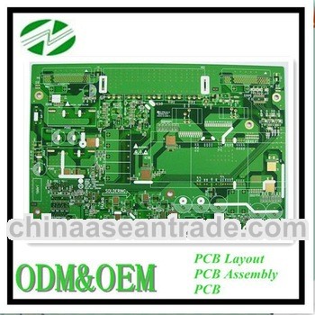
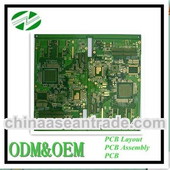
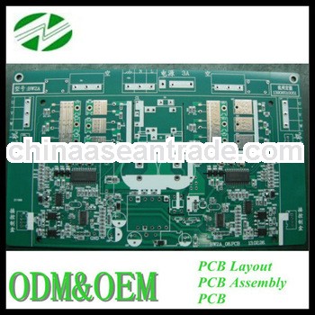
Wifi radio receiver intenet radio pcb design
One-stop pcb assemblies service, We can offer 1 to 12 Layer PCB fabrication, PCB design, PCB layout, PCB manufacturing, PCB Assemblies, components sourcing, PCBA Function Test, design solution.
Item | Manufacture Capability | |
Material | FR-4 / Hi Tg FR-4 / Lead free Materials (RoHS Compliant) /CEM-3, Aluminium, Metal based | |
Layer No. | 1-16 | |
Finished Board thickness | 0.2 mm-3.8mm’(8 mil-150 mil) | |
| ||
Board Thickness Tolerance | ±10% | |
Cooper thickness | 0.5 OZ-11OZ (18 um-385 um) | |
Copper Plating Hole | 18-40 um | |
Impedance Control | ±10% | |
Warp&Twist | 0.70% | |
Peelable | 0.012"(0.3mm)-0.02’(0.5mm) | |
Images | ||
Min Trace Width (a) | 0.1mm (4 mil) |
|
Min Space Width (b) | 0.1mm (4 mil) | |
Min Annular Ring | 0.1mm (4 mil) |
|
SMD Pitch (a) | 0.2 mm(8 mil) |
|
BGA Pitch (b) | 0.2 mm (8 mil) | |
|
| |
Solder Mask | ||
Min Solder Mask Dam (a) | 0.0635 mm (2.5mil) |
|
Soldermask Clearance (b) | 0.1mm (4 mil) | |
Min SMT Pad spacing (c) | 0.1mm (4 mil) | |
Solder Mask Thickness | 0.0007"(0.018mm) | |
Holes | ||
Min Hole size (CNC) | 0.2 mm (8 mil) | |
Min Punch Hole Size | 0.9 mm (35 mil) | |
Hole Size Tol (+/-) | PTH:±0.075mm;NPTH: ±0.05mm | |
Hole Position Tol | ±0.075mm | |
Plating | ||
HASL | 2.5um | |
Lead free HASL | 2.5um | |
Immersion Gold | Nickel 3-7um Au:1-5u'' | |
OSP | 0.2-0.5um | |
Outline | ||
Panel Outline Tol (+/-) | CNC: ±0.125mm, Punching: ±0.15mm | |
Beveling | 30°45° | |
Gold Finger angle | 15° 30° 45° 60° | |
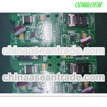
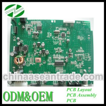
Electronic PCBA products
We supply complete PCB Assembly services including PCB & material purchasing, SMT, testing, packing, delivery.
We offer good quality warrantee, shipping lead time guarantee and lower price guarantee for all over the world.
After we get customers' product design idea(ODM)/ Gerber file & BOM list(OEM), we could offer full PCB Assembly services as below:
1 Product design and development;
2 PCB making according to PCB design;
3 Material Purchasing as BOM offered;
5 SMT/Through hole assembly;
6 Testing;
Inside circuit testing finds out every problem from manufacturing or material itself.
7 Boards cleaning;
8 Mechanism Assembly;
9 Packaging: Burble bags & seperate box /carton
10 Quick &Safe Delivery.
SMT Production Flow:
Material Receiving → IQC → Stock → Material to SMT → SMT Line Loading → Solder Paste/Glue Printing → Chip Mount → Reflow → 100% Visual Inspection → Automated Optical Inspection (AOI) → SMT QC Sampling → SMT Stock → Material to PTH → PTH Line Loading → Plated Through Hole → Wave Soldering → Touch Up → 100% Visual Inspection → PTH QC Sampling → In-Circuit Test (ICT) → Final Assembly → Functional Test (FCT) → Packing → OQC Sampling → Shipping
Available service :
1.Research and manufacture electronical products
2. PCB production service.
3. PCB assembly service. Available on SMT, BGA, DIP.
4. high quality led lights towards hight-end markets.Available on highbay light and panel light
5. Electronic Component purchasing service
Lead time of prototype:
1. 10-15days, with customers completed technical information.
2. 12-18days, with customers samples
3. 20-25days, with customers request and our new design
Production period: 15-20days (5 more days for trial order)
We customize various LED dimmer as per customer's requirements. If you are interested, pls feel free to contact me.
If you send us your Gerber Files and PCB specifications, we will quote for you within 12 hours
We always try our best! So we do, we conquer, and we get there!
Try us!